Huawei now says it can build 1.4nm-class chips without ASML's most advanced machines
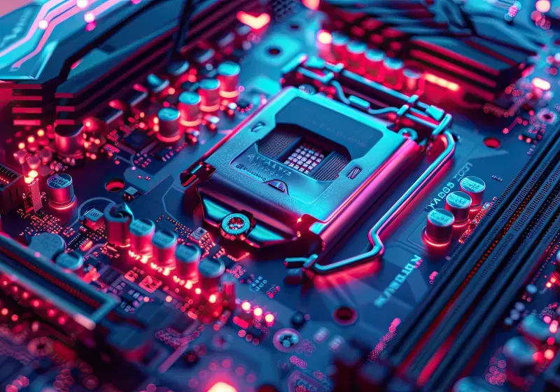
Huawei Technologies announced it is developing a method to produce chips with transistor densities comparable to a 1.4‑nanometer process without using ASML’s extreme ultraviolet lithography machines. The approach relies on stacking multiple circuit layers and a design framework called LogicFolding, which will be used in upcoming Kirin smartphone chips. Industry analysts view the effort as a notable but unproven alternative to traditional chip manufacturing amid ongoing US export restrictions.
- ▪Huawei says its new architecture can achieve 1.4nm‑class density by 2031 using stacked layers and advanced packaging.
- ▪The company has been blocked from accessing ASML equipment due to US export controls and has spent six years refining its semiconductor capabilities.
- ▪Huawei has already mass‑produced 381 chip models using related techniques, but independent performance data against rivals is not yet available.
- ▪Analysts note challenges such as heat management and increased design complexity that must be resolved before large‑scale deployment.
TechSpot files mainly under tech. We currently carry 379 of its stories.
Story provenance
Source · retrieval · rights · ranking — open for full record
inspect →
Story provenance
Attribution is not the same as permission. This drawer separates discovery metadata, excerpts, WeSearch-generated summaries, reuse status, and whether the publisher receives the visit. Nothing here claims a legal grant the publisher has not made.
Record
| Original publisher | TechSpot |
| Canonical URL | https://www.techspot.com/news/112519-huawei-now-can-build-14nm-class-chips-without.html |
| Publication time | Mon, 25 May 2026 07:49 -0500 |
| Retrieval time | 2026-05-25T12:52:36.700Z |
| Last seen | 2026-05-25T12:52:37.938Z |
| Headline source | Publisher (no WeSearch rewrite) |
| Excerpt source | publisher body |
| Excerpt method | First ~120 words (~800 chars) of extracted publisher body, fair-use limited. |
| Summary | WeSearch · cerebras-chat (WeSearch summarizer) |
| Summary source text | contentText |
| Citation coverage | Summary is a WeSearch-generated derivative; primary citation is the original publisher URL. |
| Cluster | xQUxu1soDBv9 |
| Cluster logic | Grouped by semantic title/content similarity across sources within a rolling window. Same-publisher template collisions are excluded from coverage comparison. |
| Ranking reason | Story pages are not engagement-ranked. Hub feeds use recency, with optional source-diversified chronological ordering (cap consecutive stories per source). No personalized ranking. |
| Publisher visit | Yes — open original |
| Substitutes article? | No — link-out required for full text |
Rights status (four layers)
WeSearch handling by dimension
| Indexing | May the item be indexed (stored, ranked, made findable)? | Allowed |
| Snippet | May a short excerpt of the publisher's text be shown? | Allowed |
| AI summary | May WeSearch generate its own short summary of the article? | Limited |
| Retrieval / RAG | May the content be exposed for third-party retrieval-augmented generation? | Not asserted |
| Model training | May the content be used to train AI models? | Not asserted |
| Commercial reuse | May the content be reused commercially? | Not permitted |
Basis: Derived from the published RSS/Atom feed. Contact: [email protected]. Reviewed: 2026-07-24.
Opening excerpt (first ~120 words) tap to expand
Hardware Industry chip huawei Huawei says it can build 1.4nm chips without ASML's most advanced machines Cut off from advanced lithography tools, Huawei is betting on stacked chip architectures and new packaging methods By Skye Jacobs May 25, 2026, 7:49 10 comments Serving tech enthusiasts for over 25 years. TechSpot means tech analysis and advice you can trust. What we know so far: Huawei Technologies is betting it can sidestep one of the semiconductor industry's most entrenched dependencies: the need for cutting-edge lithography machines. The company says it has developed a way to build advanced chips without access to the specialized equipment that has long defined the global pecking order in chipmaking.
…
Excerpt limited to ~120 words for fair-use compliance. The full article is at TechSpot.
Discussion
0 commentsMore from TechSpot