Through-Glass Vias and the Long Road to Glass Substrates
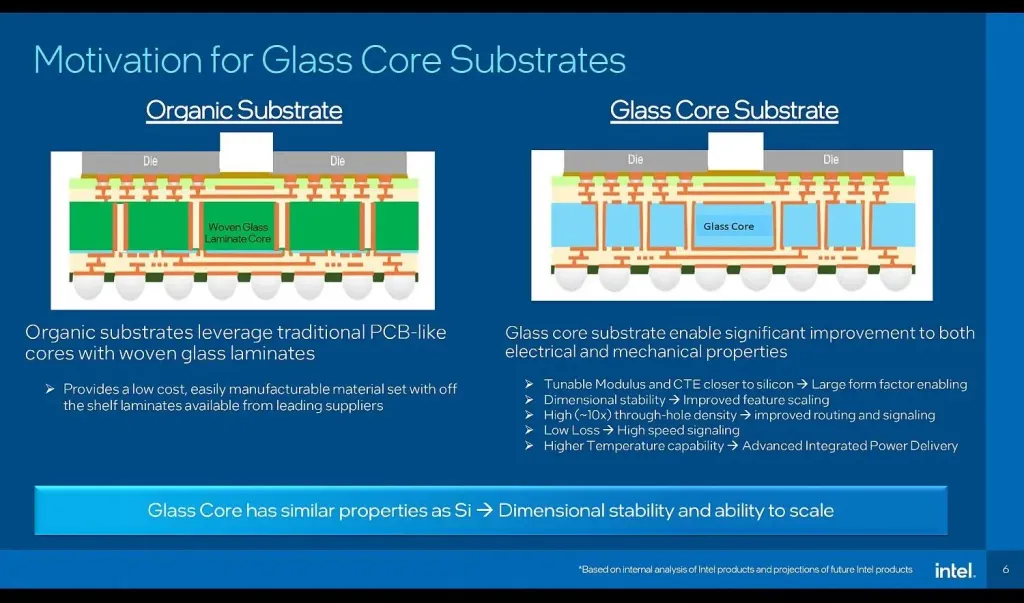
Glass-based substrates are gradually replacing organic substrates in PCBs due to their superior properties. However, challenges remain in creating through-glass vias (TGVs) that are defect-free and properly coated with copper. The advantages of glass substrates extend beyond chip packaging, making them suitable for advanced sensors and communication devices.
- ▪Glass substrates are beginning to replace organic substrates in PCBs due to better material properties.
- ▪Creating defect-free through-glass vias is a significant challenge that requires precise laser drilling techniques.
- ▪Glass substrates offer advantages such as chemical resistance, higher heat resistance, and transparency to RF.
Hackaday files mainly under tech. We currently carry 211 of its stories.
Story provenance
Source · retrieval · rights · ranking — open for full record
inspect →
Story provenance
Attribution is not the same as permission. This drawer separates discovery metadata, excerpts, WeSearch-generated summaries, reuse status, and whether the publisher receives the visit. Nothing here claims a legal grant the publisher has not made.
Record
| Original publisher | Hackaday |
| Canonical URL | https://hackaday.com/2026/05/25/through-glass-vias-and-the-long-road-to-glass-substrates/ |
| Publication time | Tue, 26 May 2026 02:00:00 +0000 |
| Retrieval time | 2026-05-26T02:02:41.705Z |
| Last seen | 2026-05-26T02:02:41.705Z |
| Headline source | Publisher (no WeSearch rewrite) |
| Excerpt source | publisher body |
| Excerpt method | First ~120 words (~800 chars) of extracted publisher body, fair-use limited. |
| Summary | WeSearch · cerebras-chat (WeSearch summarizer) |
| Summary source text | contentText |
| Citation coverage | Summary is a WeSearch-generated derivative; primary citation is the original publisher URL. |
| Cluster | TNopNuNye-YW |
| Cluster logic | Grouped by semantic title/content similarity across sources within a rolling window. Same-publisher template collisions are excluded from coverage comparison. |
| Ranking reason | Story pages are not engagement-ranked. Hub feeds use recency, with optional source-diversified chronological ordering (cap consecutive stories per source). No personalized ranking. |
| Publisher visit | Yes — open original |
| Substitutes article? | No — link-out required for full text |
Rights status (four layers)
WeSearch handling by dimension
| Indexing | May the item be indexed (stored, ranked, made findable)? | Allowed |
| Snippet | May a short excerpt of the publisher's text be shown? | Allowed |
| AI summary | May WeSearch generate its own short summary of the article? | Limited |
| Retrieval / RAG | May the content be exposed for third-party retrieval-augmented generation? | Not asserted |
| Model training | May the content be used to train AI models? | Not asserted |
| Commercial reuse | May the content be reused commercially? | Not permitted |
Basis: Derived from the published RSS/Atom feed. Contact: [email protected]. Reviewed: 2026-07-24.
Opening excerpt (first ~120 words) tap to expand
Through-Glass Vias And The Long Road To Glass Substrates No comments by: Maya Posch May 25, 2026 Title: Copy Short Link: Copy Credit: Keith Best, Semiengineering. Glass-based substrates are slowly beginning to push out organic substrates commonly used in PCBs due to often superior material properties. One area where glass substrates have however struggled is with through-hole vias and providing the conductive copper path through them. A 2024 article by [Keith Best] gives a good overview of the topic, with recent news showing how much companies like Intel are pushing for glass substrates, specifically for the packaging of dies. One major advantage with vias in glass substrates is that they can be much smaller, enabling smaller than 0.1 mm diameter holes with far finer pitch.
…
Excerpt limited to ~120 words for fair-use compliance. The full article is at Hackaday.
Discussion
0 commentsMore from Hackaday