Using Azo Photoisomerization to Alter Semiconductor Film Properties
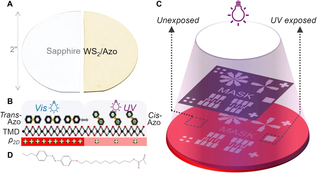
Researchers have demonstrated that azobenzene compounds can optically alter the properties of semiconductor films when exposed to UV light. This technique allows for dynamic changes in carrier densities within transition metal dichalcogenide monolayers, effectively modifying the behavior of field-effect transistors. The proof-of-concept study suggests potential applications in developing programmable circuits and sensors that respond to external stimuli.
- ▪Exposing azobenzene compounds to UV light enables the optical alteration of semiconductor film properties.
- ▪The study utilized a transition metal dichalcogenide monolayer combined with the Azo compound to create a functional device.
- ▪Visible and UV light were used to alter carrier densities in both n-type and p-type FET semiconductors.
- ▪The research was published in Science Advances and covered by Princeton University.
- ▪This method offers a pathway to creating semiconductor devices whose behavior dynamically changes in response to electromagnetic radiation or temperature.
Hackaday files mainly under tech. We currently carry 395 of its stories.
Story provenance
Source · retrieval · rights · ranking — open for full record
inspect →
Story provenance
Attribution is not the same as permission. This drawer separates discovery metadata, excerpts, WeSearch-generated summaries, reuse status, and whether the publisher receives the visit. Nothing here claims a legal grant the publisher has not made.
Record
| Original publisher | Hackaday |
| Canonical URL | https://hackaday.com/2026/09/19/using-azo-photoisomerization-to-alter-semiconductor-film-properties/ |
| Publication time | Sat, 19 Sep 2026 11:00:40 +0000 |
| Retrieval time | 2026-09-19T11:03:47.102Z |
| Last seen | 2026-09-19T11:03:47.102Z |
| Headline source | Publisher (no WeSearch rewrite) |
| Excerpt source | publisher body |
| Excerpt method | First ~120 words (~800 chars) of extracted publisher body, fair-use limited. |
| Summary | WeSearch · cerebras-chat (WeSearch summarizer) |
| Summary source text | contentText |
| Citation coverage | Summary is a WeSearch-generated derivative; primary citation is the original publisher URL. |
| Cluster | o0QHFzQB7FV_ · 1 stories |
| Cluster logic | Grouped by semantic title/content similarity across sources within a rolling window. Same-publisher template collisions are excluded from coverage comparison. |
| Ranking reason | Story pages are not engagement-ranked. Hub feeds use recency, with optional source-diversified chronological ordering (cap consecutive stories per source). No personalized ranking. |
| Publisher visit | Yes — open original |
| Substitutes article? | No — link-out required for full text |
Rights status (four layers)
WeSearch handling by dimension
| Indexing | May the item be indexed (stored, ranked, made findable)? | Allowed |
| Snippet | May a short excerpt of the publisher's text be shown? | Allowed |
| AI summary | May WeSearch generate its own short summary of the article? | Limited |
| Retrieval / RAG | May the content be exposed for third-party retrieval-augmented generation? | Not asserted |
| Model training | May the content be used to train AI models? | Not asserted |
| Commercial reuse | May the content be reused commercially? | Not permitted |
Basis: Derived from the published RSS/Atom feed. Contact: [email protected]. Reviewed: 2026-07-24.
Opening excerpt (first ~120 words) tap to expand
Using Azo Photoisomerization To Alter Semiconductor Film Properties No comments by: Maya Posch September 19, 2026 Title: Copy Short Link: Copy Generally semiconductor devices like transistors have fixed properties, but using an azobenzene (Azo) compound it’s possible to optically alter these properties by exposing them to UV light. This is demonstrated in a recent paper by [Jaehoon Ji] et al., as published in Science Advances, with accompanying coverage by Princeton University. Building on previous research on e.g. flakes of MoS2 with photochromic Azo molecules, a functional semiconductor device was created. This uses a transition metal dichalcogenide (TMD) monolayer combined with the Azo compound, with the latter altering the electrical and optical properties of the structure.
…
Excerpt limited to ~120 words for fair-use compliance. The full article is at Hackaday.
Discussion
0 commentsMore from Hackaday